- 您现在的位置:买卖IC网 > Sheet目录366 > TMDXEVM5515 (Texas Instruments)EVAL MODULE DSP FOR C55XX
SPRS645F – AUGUST 2010 – REVISED OCTOBER 2013
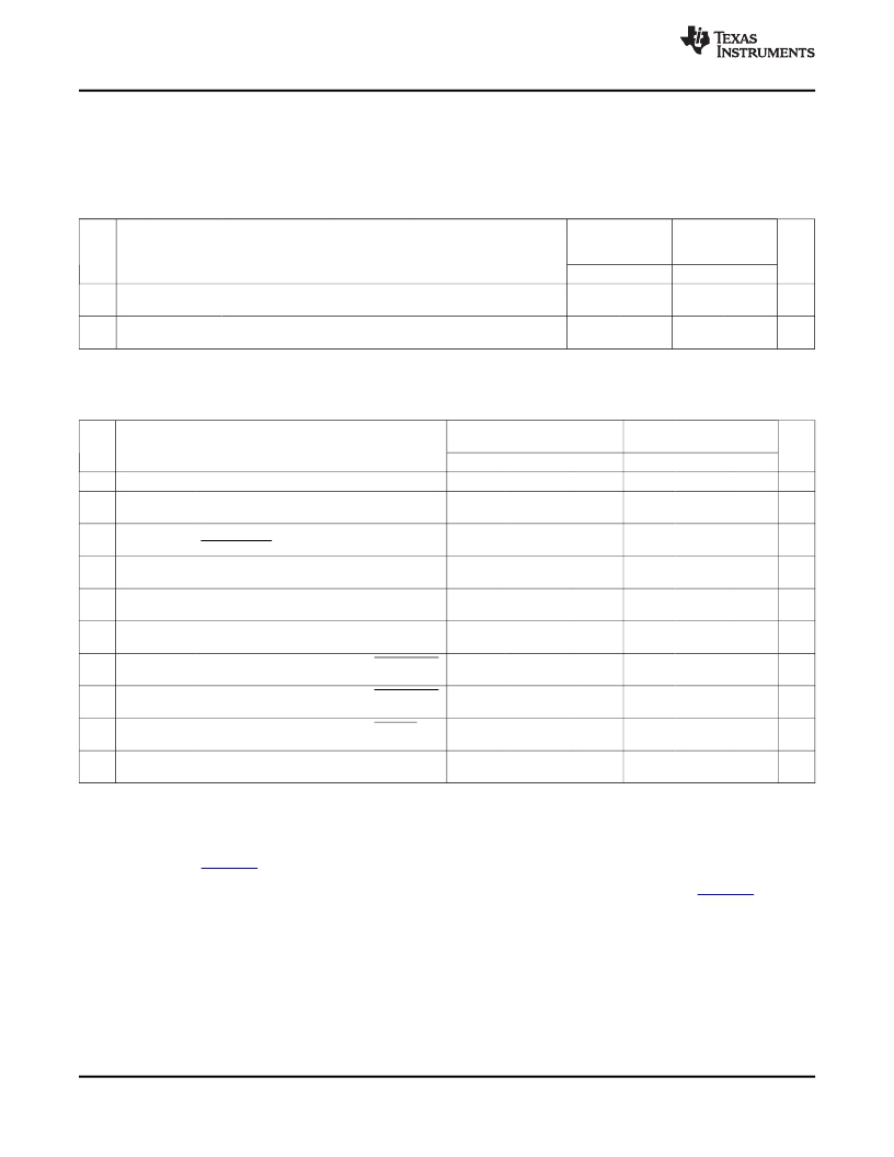
5.9.5
EMIF Electrical Data/Timing CV DD = 1.3 V, DV DDEMIF = 3.3/2.75/2.5/1.8 V, External
Loading = 10 pF
NO.
CV DD = 1.3 V
DV DDEMIF =
3.3/2.75/2.5 V
CV DD = 1.3 V
DV DDEMIF = 1.8 V
UNIT
MIN
MAX
MIN
MAX
19
20
t su(DV-CLKH)
t h(CLKH-DIV)
Input setup time, read data valid on EM_D[15:0] before
EM_SDCLK rising
Input hold time, read data valid on EM_D[15:0] after EM_SDCLK
rising
3.4
1.2
3.4
1.2
ns
ns
(1)
Timing parameters are obtained with 10pF loading on the EMIF pins.
Table 5-17. Switching Characteristics Over Recommended Operating Conditions for EMIF
CV DD = 1.3 V
CV DD = 1.3 V
NO.
PARAMETER
DV DDEMIF = 3.3/2.75/2.5 V
DV DDEMIF = 1.8 V
UNIT
MIN
NOM
MAX
MIN
NOM
MAX
1
2
t c(CLK)
t w(CLK)
Cycle time, EMIF clock EM_SDCLK
Pulse width, EMIF clock EM_SDCLK high or
low
10 (3)
5
20 (4)
10
ns
ns
3
5
7
9
11
13
15
21
t d(CLKH-CSV)
t d(CLKH-DQMV)
t d(CLKH-AV)
t d(CLKH-DV)
t d(CLKH-RASV)
t d(CLKH-CASV)
t d(CLKH-WEV)
t d(CLKH-CKEV)
Delay time, EM_SDCLK rising to
EMA_CS[1:0] valid
Delay time, EM_SDCLK rising to
EM_DQM[1:0] valid
Delay time, EM_SDCLK rising to EM_A[20:0]
and EM_BA[1:0] valid
Delay time, EM_SDCLK rising to EM_D[15:0]
valid
Delay time, EM_SDCLK rising to EM_SDRAS
valid
Delay time, EM_SDCLK rising to EM_SDCAS
valid
Delay time, EM_SDCLK rising to EM_WE
valid
Delay time, EM_SDCLK rising to EM_SDCKE
valid
1.1
1.1
1.1
1.1
1.1
1.1
1.1
1.1
7.77
7.77
7.77
7.77
7.77
7.77
7.77
7.77
1.1
1.1
1.1
1.1
1.1
1.1
1.1
1.1
7.77
7.77
7.77
7.77
7.77
7.77
7.77
7.77
ns
ns
ns
ns
ns
ns
ns
ns
(1)
(2)
(3)
(4)
Timing parameters are obtained with 10pF loading on the EMIF pins.
E = SYSCLK period in ns. For example, when SYSCLK is set to 60 or 100 MHz, E = 16.67 or 10 ns, respectively. For more detail on the
EM_SDCLK speed see Section 5.9.2 , EMIF Non-Mobile and Mobile Synchronous DRAM Memory Supported .
When CV DD = 1.3 V, and DV DDEMIF = 3.3 V, 2.75 V or 2.5 V, the max clock frequency on the EM_SDCLK pin is limited to 100 MHz
(EM_SDCLK = 100 MHz). For more information, see TMS320C5515/14/05/04 DSP External Memory Interface (EMIF) User's Guide
(literature number SPRUGU6 ).
When DV DDEMIF = 1.8 V, the max clock frequency on the EM_SDCLK pin is limited to 50 MHz (EM_SDCLK = 50 MHz). For more
information, see TMS320C5515/14/05/04 DSP External Memory Interface (EMIF) User's Guide (literature number SPRUGU6 ).
96
Peripheral Information and Electrical Specifications
Product Folder Links: TMS320C5515
Copyright ? 2010–2013, Texas Instruments Incorporated
发布紧急采购,3分钟左右您将得到回复。
相关PDF资料
TMDXEXP1808L
KIT EXPERIMENTER FOR AM180X
TO263-3EV-VREG
BOARD EVAL TO220-3/TO263-3 VREG
TO263-5EV-VREG
EVAL BOARD VREG TO220-5/TO263-5
TOOLSTICK-EK
KIT TOOL EVAL SYS IN A USB STICK
TPS23757EVM
EVALUATION MODULE FOR TPS23757
TPS62230EVM-370
EVAL MODULE FOR TPS62230-370
TRAVELCUBE
SURGE SUP 1OUT W/RJ11 DIRECTPLUG
TRAVELER100BT
SURGE SUP 2OUT W/RJ11 DIRECTPLUG
相关代理商/技术参数
TMDXEVM5515
制造商:Texas Instruments 功能描述:TMS320C5515 DSP Evaluation Module
TMDXEVM642
制造商:Texas Instruments 功能描述:Tools Development kit For Use
TMDXEVM6424
功能描述:开发板和工具包 - TMS320 C6424 DSP Eval Mod RoHS:否 制造商:Texas Instruments 产品:Experimenter Kits 工具用于评估:F2802x 核心:TMS320 接口类型:UART, USB 工作电源电压:
TMDXEVM6446
制造商:Rochester Electronics LLC 功能描述:DAVINCI EVM BUNDLE W/O EMULATOR - Bulk 制造商:Texas Instruments 功能描述:DAVINCI EVM BUNDLE W/O EMULATOR - Bulk
TMDXEVM6446T
制造商:Texas Instruments 功能描述:DM6446 DIGITAL VIDEO EVALUATION MODULE - Boxed Product (Development Kits)
TMDXEVM6446TS
制造商:Texas Instruments 功能描述:DM6446 DIGITAL VIDEO EVALUATION MODULE - Trays
TMDXEVM6452
功能描述:开发板和工具包 - TMS320 C6452 EVM Evaluation Module RoHS:否 制造商:Texas Instruments 产品:Experimenter Kits 工具用于评估:F2802x 核心:TMS320 接口类型:UART, USB 工作电源电压:
TMDXEVM6455
功能描述:开发板和工具包 - TMS320 C6455 Evaluation Module RoHS:否 制造商:Texas Instruments 产品:Experimenter Kits 工具用于评估:F2802x 核心:TMS320 接口类型:UART, USB 工作电源电压:
